
A new milestone for science at NTU: The inauguration of the Max Planck-IAS-NTU Center
瀏覽器版本過舊,或未開啟 javascript
請更新瀏覽器或啟用 javascript
Spotlights
Date: May 25, 2020
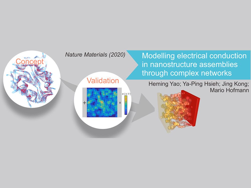
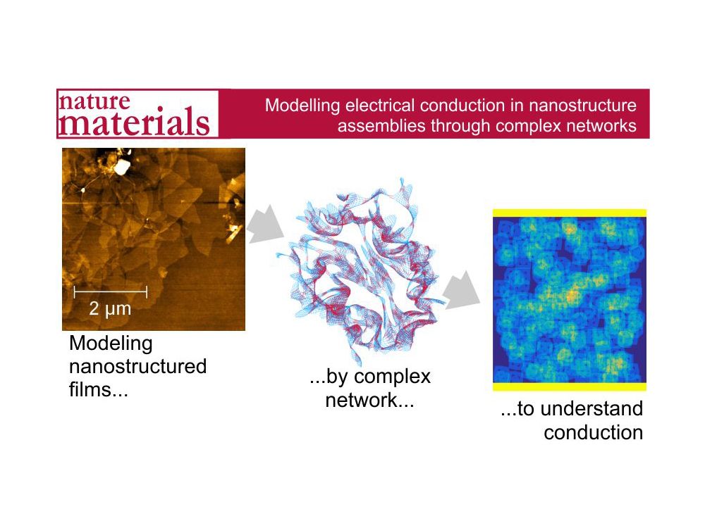
The research results of MY-Lab are published on Nature Materials.
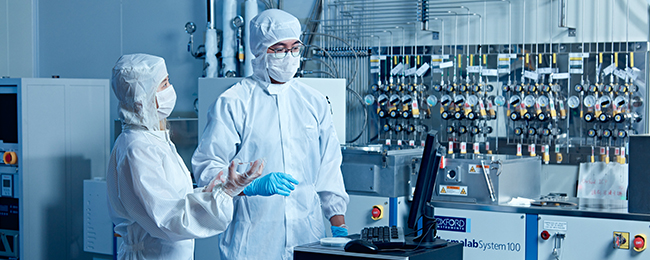
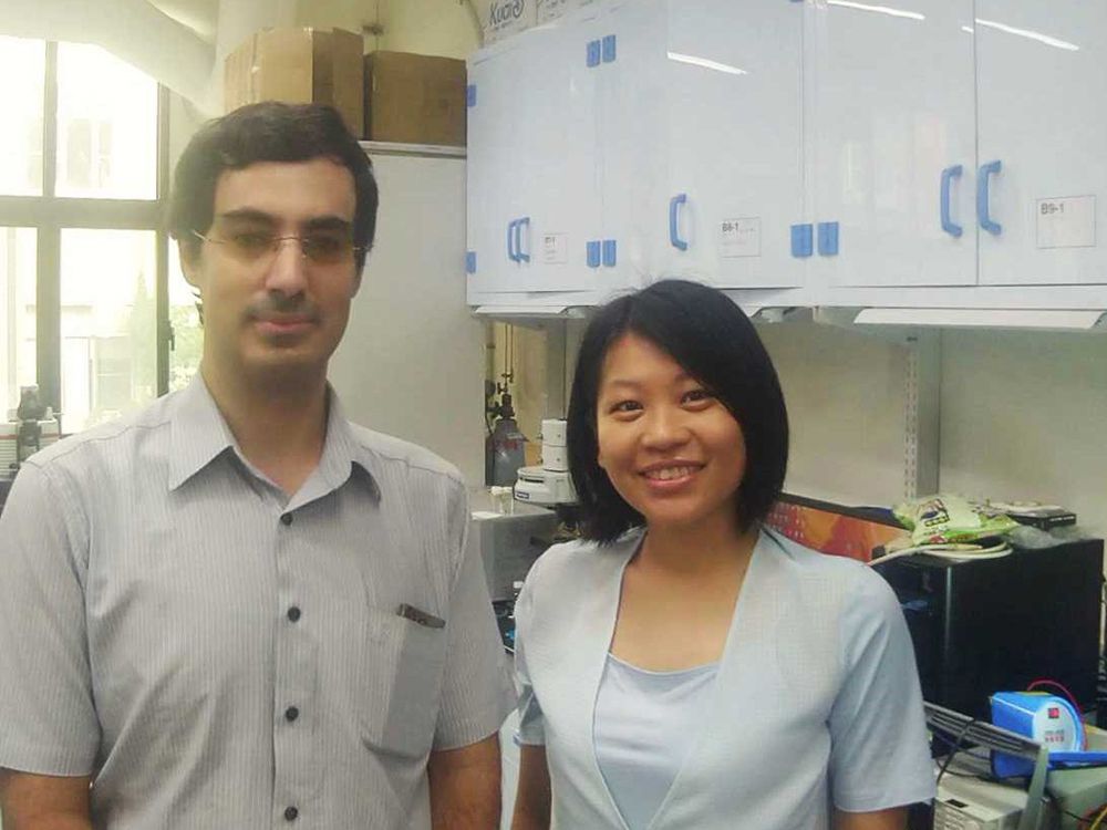
Associate Prof. Mario Hofmann (left) and Dr. Ya-Ping Hsieh (right).
This figure shows how complex networks are applied to understand and predict conduction in nanostructures.
The last 20 years have seen a revolution of nanomaterials, such as nanotubes, flakes, and buckyballs, that are composed of just a few thousand atoms. To make an impact on our macroscopic world, millions of these nanoobjects have to be combined.
Associate Prof. Mario Hofmann of NTU’s Department of Physics and Dr. Ya-Ping Hsieh (謝雅萍) of the Institute of Atomic and Molecular Sciences (IAMS) at Academia Sinica, formed MY-Lab and set to work on putting thin films of graphene flakes on glass to form invisible electrodes for screens and solar cells. This task proved more difficult than expected, as making flakes thicker would reduce transparency while making flakes larger would compromise conduction.
As the flakes were randomly shaped and oriented, the MY-Lab team had to capture the complicated conduction among different flakes by developing their own tool with the help of a visiting student from the University of Hong Kong.
Instead of describing the nanomaterial as patterned in shape to predict conduction, the team introduced a simple and universal method to convert the nanostructure into a complex network with arbitrary connectivity similar to the connections in the brain or links among websites. The links among materials and networks were made by breaking each flake into hundreds of pieces and giving each piece a resistance. This facilitated calculation with the help of a software that had been developed to predict animal migration patterns. Even without programming experience, this approach allowed researchers to capture the complexity of many nanomaterials.
Returning to their original task, the researchers were able to connect their results with simulations in nanostructured films and extract important information. By comparing two simple measurements (i.e., light absorption and film resistance) of a sample to the simulation results, the team could estimate the properties of a single flake. This approach allowed the researchers to compare different films and materials to obtain the optimal electrode or transistor without having to use high-powered microscopes or specialized measurement tools.
Finally, the team investigated 200 different types of nanostructures to determine which geometry would be the most suitable for their electrodes, and was reassured to find that flakes are close to ideal for this application.
Their work has recently been published in Nature Materials under the title of “Modelling Electrical Conduction in Nanostructure Assemblies through Complex Networks” (April 20, 2020), and the authors hope that researchers in the field of materials science and nanotechnology will be inspired to use their method for improving our understanding of the unexpected properties of nanostructures.
This article is also featured in No. 78 of NTU Highlights (June 2020).
A new milestone for science at NTU: The inauguration of the Max Planck-IAS-NTU Center
A Distinguished Global Research Center Established at NTU under Trilateral Cooperation
Collaborative study between NTU and Japan uncovers the origin of Adzuki Beans and agriculture in Japan
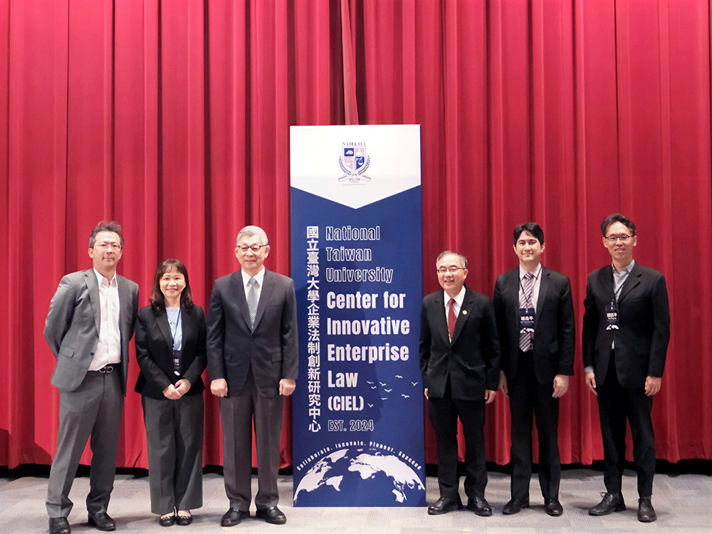
NTU Launches Center for Innovation in Enterprise Law—with Forum Highlighting Trump’s Policy and Legal Shifts Amid Geopolitical Tensions
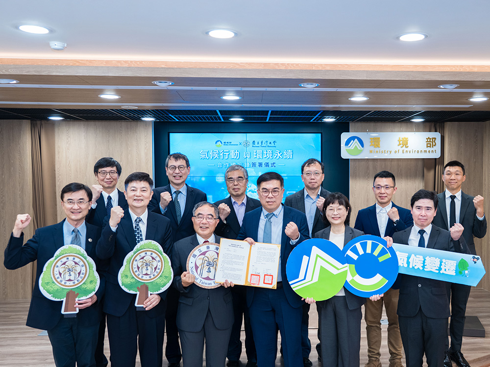
NTU and Ministry of Environment Sign MOU to Advance Net-Zero Transition and Environmental Resilience
Current Spotlights
A new milestone for science at NTU: The inauguration of the Max Planck-IAS-NTU Center
A Distinguished Global Research Center Established at NTU under Trilateral Cooperation
Collaborative study between NTU and Japan uncovers the origin of Adzuki Beans and agriculture in Japan
NTU Launches Center for Innovation in Enterprise Law—with Forum Highlighting Trump’s Policy and Legal Shifts Amid Geopolitical Tensions
NTU and Ministry of Environment Sign MOU to Advance Net-Zero Transition and Environmental Resilience