
A new milestone for science at NTU: The inauguration of the Max Planck-IAS-NTU Center
瀏覽器版本過舊,或未開啟 javascript
請更新瀏覽器或啟用 javascript
Spotlights
Date: May 14, 2021
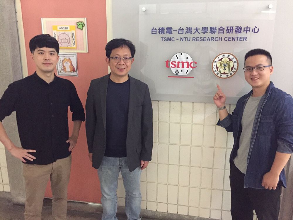
NTU, TSMC and MIT’s international collaboration culminates in research article published in Nature (left to right: Dr. Pin-Chun Shen, Prof. Chih-I Wu, Dr. Ang-Sheng Chou).
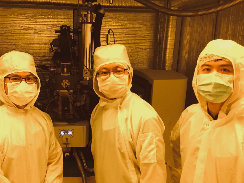
Research team and the helium-ion beam lithography system (left to right: Dr. Ang-Sheng Chou, Prof. Chih-I Wu, Dr. Pin-Chun Shen).
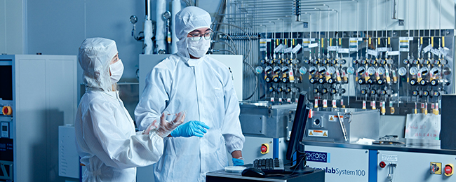
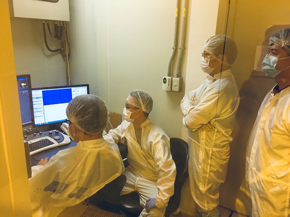
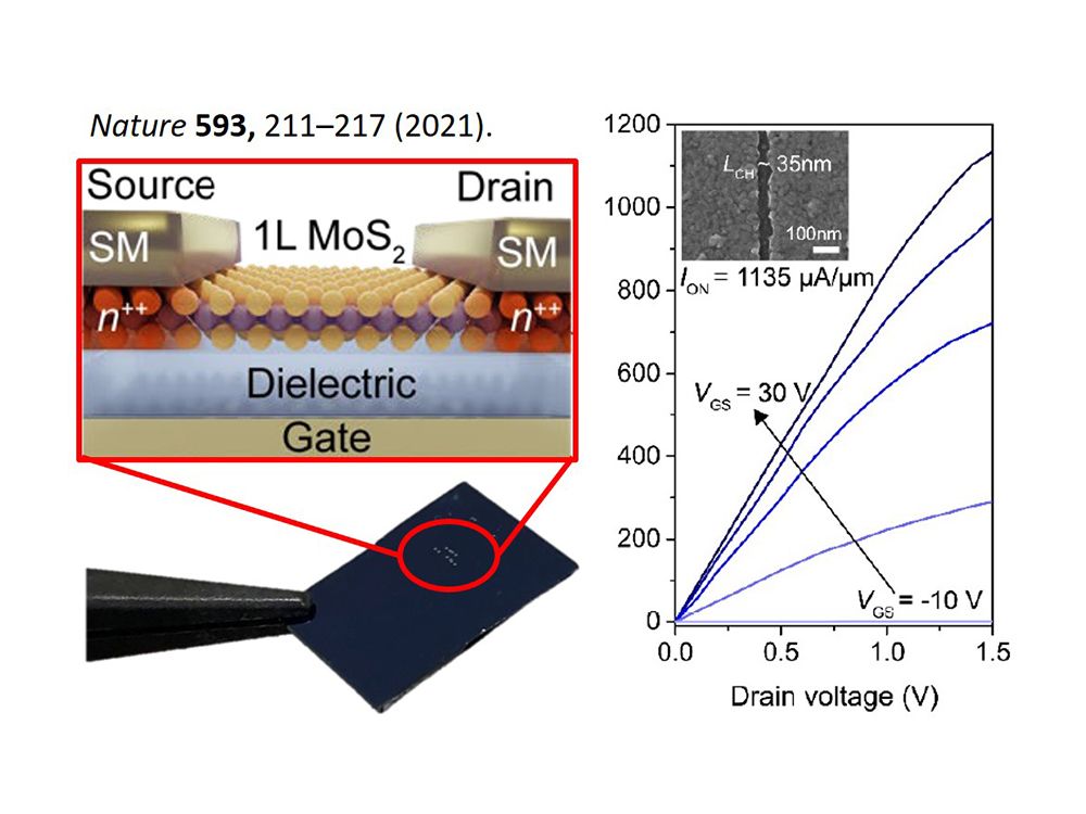
The system that helped to conclude the research on nanoscale transistors: Helium-ion beam lithography and its supporting environment .
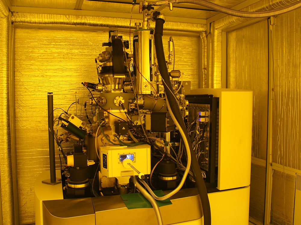
Helium-ion beam lithography system.
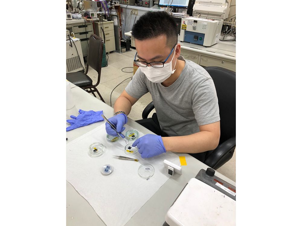
Transfer of two-dimensional material.
Device structure and its electrical properties.
A global leader in semiconductor manufacturing, Taiwan is constantly pursuing the challenge of achieving the ultimate in scaling limits. As silicon-based semiconductors are fast closing in on the physical limits of matter, the global scientific community has been actively on the hunt for alternative materials to replace silicon. Research conducted by NTU in collaboration with Taiwan Semiconductor Manufacturing Co., Ltd. (TSMC) and Massachusetts Institute of Technology (MIT) has discovered that two-dimensional materials combined with semimetallic bismuth are capable of achieving extremely low resistance that approaches the quantum limit, which will be helpful in achieving the difficult challenge of realizing sub-1nm semiconductors. The results of their research have been published in the scientific journal Nature.
Currently mainstream silicon-based semiconductor manufacturing processes have advanced to the 5-nm and 3-nm nodes. The transistor count per unit area of the wafer is approaching the physical limit of silicon, the principal material used in current semiconductor manufacturing. The scientific community has always had high hopes for two-dimensional materials but has been unable to solve the high-resistance and low-current problems associated with two-dimensional materials. The dream of replacing silicon with these novel, potential semiconductor materials has been largely out of reach.
The research paper jointly published by NTU, TSMC and MIT began with the discovery by the MIT team that the combination of semimetallic bismuth (Bi) electrodes with two-dimensional materials can significantly reduce resistance and increase current conduction. This was followed by the optimization of the Bi deposition process carried out by TSMC’s Corporate Research. The NTU team then employed helium-ion beam lithography to successfully reduce the channel widths of the devices down to nanoscale, and breakthrough was finally achieved.
Prof. Chih-I Wu (吳志毅) of the Dept. of Electrical Engineering and the Graduate Institute of Photonics and Optoelectronics at NTU further explained that the research discovered that with the use of Bi contact electrode as the key structure, the performance of two-dimensional transistors is not only comparable to that of silicon-based semiconductors, but also has the potential to be compatible with the mainstream silicon-based manufacturing process technology currently in operation, which may help circumvent the limitations of Moore’s law going forward. Although still at an early stage of development, this new discovery may provide excellent conditions for the creation of next-generation wafers, including low power consumption and high speed, which can be deployed in emerging technological applications that will greatly benefit the general public, such as artificial intelligence, electric vehicles, and predicting diseases.
The international collaboration efforts began in 2019 and lasted for a year and a half, and researchers from NTU, TSMC and MIT contributed to the discovery of this new path toward the future of the semiconductor industry. Two of the young PhDs involved in the project and the paper’s publication are former students at the Graduate Institute of Photonics and Optoelectronics at NTU.
Dr. Pin-Chun Shen (沈品均), an MIT graduate, is the first author and corresponding author of this research paper. According to Dr. Shen, three-dimensional materials that were used to manufacture semiconductors in the past reached the 3-nm node in terms of their physical properties and device structures. In this study, the use of two-dimensional materials allows the semiconductor’s thickness to be within 1 nm (i.e., 1 to 3 layers of atoms), which approaches the limit of how thin solid-state semiconductor materials can be. The properties of semimetallic Bi allow the energy barrier at its interface with the two-dimensional semiconductor to be eliminated, with the atomic structure of the two-dimensional semiconductor remaining intact while semimetallic Bi is being deposited.
At NTU, Prof. Chih-I Wu and Dr. Ang-Sheng Chou (周昂昇), also from the Graduate Institute of Photonics and Optoelectronics, participated in the research and co-authored the paper. According to Dr. Chou, the research team at NTU was mainly responsible for the development of nanoscale devices, and thanks to the University-Industry Collaboration Project, which is supported by both TSMC and the Ministry of Science and Technology (MOST), the opportunity of collaborating with MIT on this international project became a reality. The NTU team was able to communicate with top scholars during the collaboration. As researchers worked in different time zones, they made every second count during every discussion, whether it was conducted via email or over the phone. In retrospect, it was a very valuable experience in Dr. Chou’s academic career.
TSMC has had a long history of collaboration with NTU. Derek Lin (林春榮), the company’s deputy director of technology research organization and also deputy director of the TSMC-NTU Research Center, said that scientific research drives industrial development. TSMC has been committed to R&D and promoting innovation over the years, and the company will continue to work with top universities across the world in this endeavor. The results of the NTU-TSMC-MIT collaboration have once again demonstrated the importance of industry-academia cooperation.
Speaking in a reflective mood, Prof. Chih-I Wu concluded that universities do play a very important role in advanced international research collaborations such as this one. The helium-ion beam lithography system, the only one of its kind in Taiwan and now housed in E. E. Building No. 2 at NTU, cost tens of millions of NT dollars in investment but was instrumental in concluding the research. NTU is truly grateful to MOST and TSMC for their support and will be more than happy to collaborate with domestic and international companies. A commercial breakthrough in the future, if achieved, will help Taiwan’s semiconductor industry and technology supply chain maintain their leading positions in the world.
Nature article: https://www.nature.com/articles/s41586-021-03472-9
A new milestone for science at NTU: The inauguration of the Max Planck-IAS-NTU Center
A Distinguished Global Research Center Established at NTU under Trilateral Cooperation
Collaborative study between NTU and Japan uncovers the origin of Adzuki Beans and agriculture in Japan
NTU Launches Center for Innovation in Enterprise Law—with Forum Highlighting Trump’s Policy and Legal Shifts Amid Geopolitical Tensions
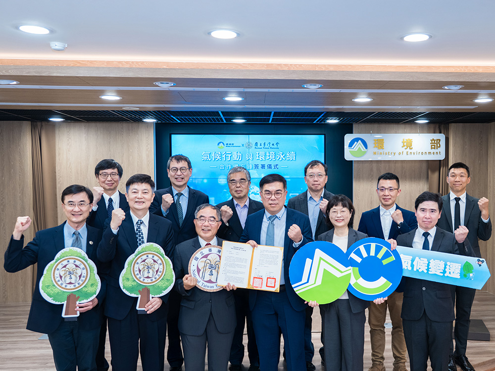
NTU and Ministry of Environment Sign MOU to Advance Net-Zero Transition and Environmental Resilience
Current Spotlights
A new milestone for science at NTU: The inauguration of the Max Planck-IAS-NTU Center
A Distinguished Global Research Center Established at NTU under Trilateral Cooperation
Collaborative study between NTU and Japan uncovers the origin of Adzuki Beans and agriculture in Japan
NTU Launches Center for Innovation in Enterprise Law—with Forum Highlighting Trump’s Policy and Legal Shifts Amid Geopolitical Tensions
NTU and Ministry of Environment Sign MOU to Advance Net-Zero Transition and Environmental Resilience