


A new milestone for science at NTU: The inauguration of the Max Planck-IAS-NTU Center
瀏覽器版本過舊,或未開啟 javascript
請更新瀏覽器或啟用 javascript
Spotlights
Date: Oct 12, 2022
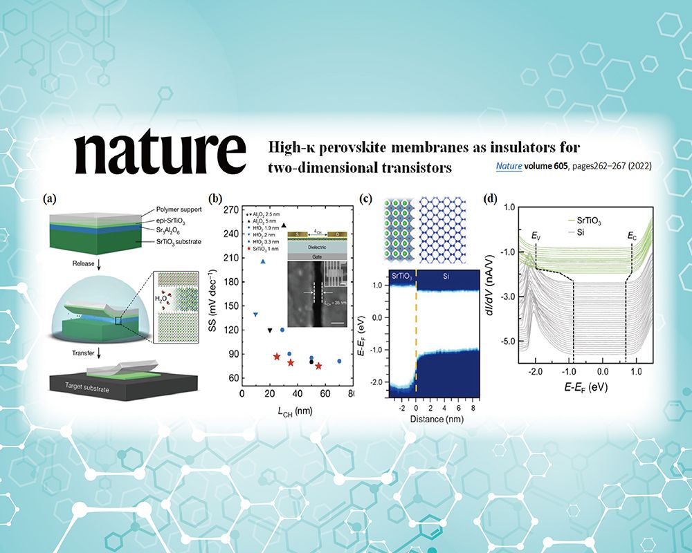
Published in Nature International Collaboration Based on Cross-Sectional STM
Professor Ya-Ping Chiu (Department of Physics, TSMC-NTU Research Center, Graduate School of Advanced Technology) and her team (graduate student Zi-Liang Yang and Dr. Bo-Chao Huang) took part as co-authors in the research of 2D layered semiconductors with cross-sectional STM conducted by Prof. Lain-Jong Li, Chair of the University of Hong Kong and Prof. Sean Li of the University of New South Wales. Their research results were published in the prestigious international journal Nature in March 2022.
As Moore’s Law continues to advance, Short-channel Effects (SCE) have become an inevitable problem in the process of continuous scaling down of transistor devices. The general method to avoid SCE is to reduce the Drain Induced Barrier Lowering (DIBL) caused by the drain, a gate oxide layer with a high dielectric constant can be adopted to increase the controllability. However, if the dielectric constant of the oxide layer is too high, it is easy for the electric field to pass through the oxide layer from the drain, resulting in the phenomenon of fringing induced barrier lowering (FIBL) caused by the marginal electric field, which weakens the performance of the device. Therefore, the current mainstream transistor gate oxide layers take advantage of hafnium dioxide (HfO2) and zirconium dioxide (ZrO2) as high dielectric constant materials (with the coefficient of κ~20-30).
The research uses transferable high dielectric perovskite strontium titanate thin film (SrTiO3, κ~270) to achieve sub-nanometer (sub-1nm) capacitance equivalent thickness (CET) of molybdenum disulfide (MoS2), as well as taking advantage of the Van der Waals gap between the molybdenum disulfide and strontium titanate thin films to change the distribution of the electric field around the drain electrode, and the influence of the energy barrier reduction effect caused by the marginal electric field is greatly reduced.
Professor Ya-Ping Chiu’s research team used cross-sectional STM to detect the high-resolution (0.2nm) electronic energy band structure at the interface of the device. By analyzing perovskite thin films (SrTiO3) and two-dimensional materials (MoS2) and the density of states between them and electrodes, they demonstrated the two-dimensional nature of the interface’s electrical properties.
This was the first time that cross-sectional STM was used to characterize two-dimensional material transistors, providing direct evidence of the electronic structure at the fundamental atomic-level interface. In the future, this key characterization technology will continue to be adopted to deal with issues related to the key interface science of low-dimensional semiconductor transistors.
Click the link to read the journal article in Nature: https://www.nature.com/articles/s41586-022-04588-2
A new milestone for science at NTU: The inauguration of the Max Planck-IAS-NTU Center
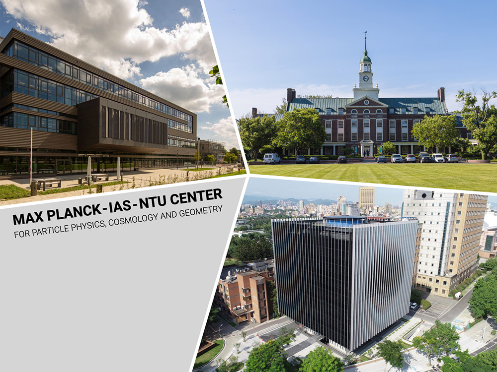
A Distinguished Global Research Center Established at NTU under Trilateral Cooperation
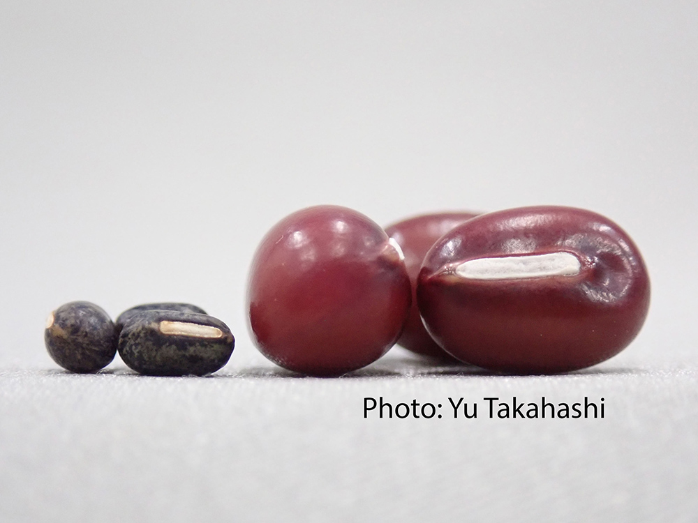
Collaborative study between NTU and Japan uncovers the origin of Adzuki Beans and agriculture in Japan
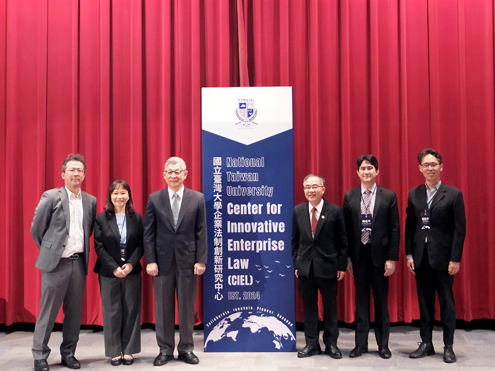
NTU Launches Center for Innovation in Enterprise Law—with Forum Highlighting Trump’s Policy and Legal Shifts Amid Geopolitical Tensions
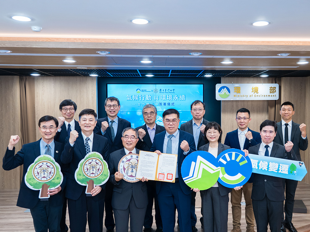
NTU and Ministry of Environment Sign MOU to Advance Net-Zero Transition and Environmental Resilience
Current Spotlights
A new milestone for science at NTU: The inauguration of the Max Planck-IAS-NTU Center
A Distinguished Global Research Center Established at NTU under Trilateral Cooperation
Collaborative study between NTU and Japan uncovers the origin of Adzuki Beans and agriculture in Japan
NTU Launches Center for Innovation in Enterprise Law—with Forum Highlighting Trump’s Policy and Legal Shifts Amid Geopolitical Tensions
NTU and Ministry of Environment Sign MOU to Advance Net-Zero Transition and Environmental Resilience