
A new milestone for science at NTU: The inauguration of the Max Planck-IAS-NTU Center
瀏覽器版本過舊,或未開啟 javascript
請更新瀏覽器或啟用 javascript
Spotlights
Date: Apr 26, 2023
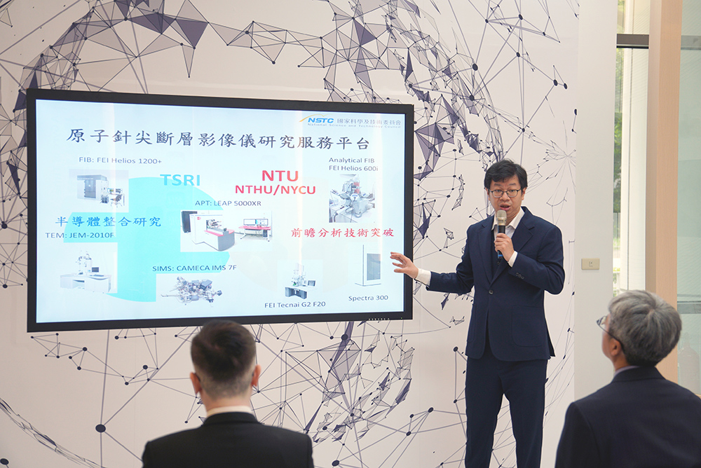
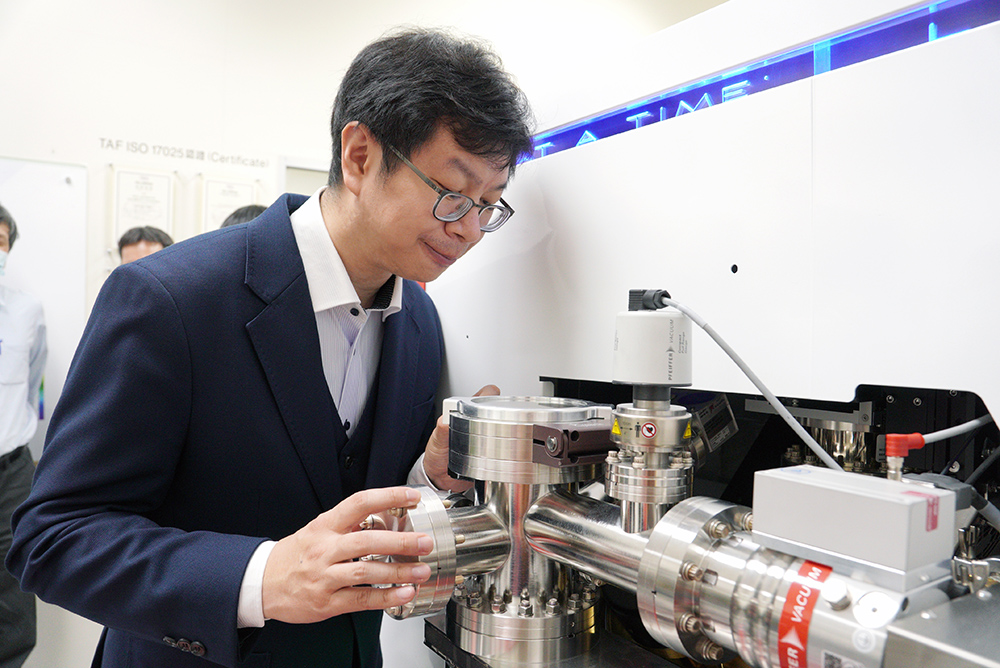
Prof. Hung-Wei Yen (顏鴻威) from the Department of Materials Science and Engineering giving a presentation about Atom Probe Tomography.
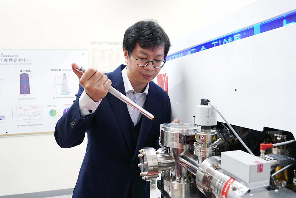
Prof. Hung-Wei Yen demonstrating APT.
Prof. Yen demonstrating APT.
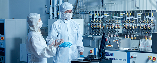
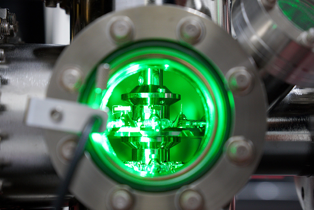
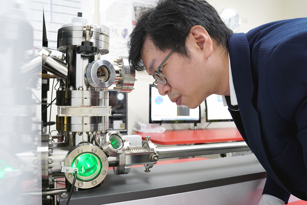
Atom Probe Tomography (APT)
Prof. Yen observing the operation of APT.
The continuous evolution of next-generation semiconductor devices requires the miniaturization of dimensions, heterogenization of materials, and three-dimensional structuring to enhance the device integration density. However, these advances also pose new challenges for material analysis techniques.
The National Science and Technology Council earlier has launched the “Breaking the Physical Limits of Semiconductors and Linking to the AI Generation” project. It plans to develop a material and device analysis technology with high resolution, high detection limits, and three-dimensional information. In this project, Taiwan Semiconductor Research Institute (TSRI), NTU, National Tsing Hua University, and Yang Ming Chiao Tung University jointly established Atom Probe Tomography (APT). The ultimate goal of this project is to accelerate the cultivation of high-level technical talents and make innovative breakthroughs in semiconductor physics.
APT is a state-of-the-art material analysis technology that allows for the atomic-scale analysis of the three-dimensional distribution of materials or devices in microscopic regions. It has a spatial resolution that can reach the atomic level, and its detection limit for concentration can be as low as 20 parts per million (ppm). APT has been applied in the microscopic analysis of materials, devices, geology, biology, and other substances. APT’s unique integration of excellent spatial resolution and composition detection limits makes it a key technology for the development of next-generation semiconductor devices. The establishment of APT in Taiwan represents a significant leap forward in semiconductor material analysis technology and signifies that Taiwan has the corresponding technological capabilities to conduct material analysis while the semiconductor industry continues to evolve.
A new milestone for science at NTU: The inauguration of the Max Planck-IAS-NTU Center
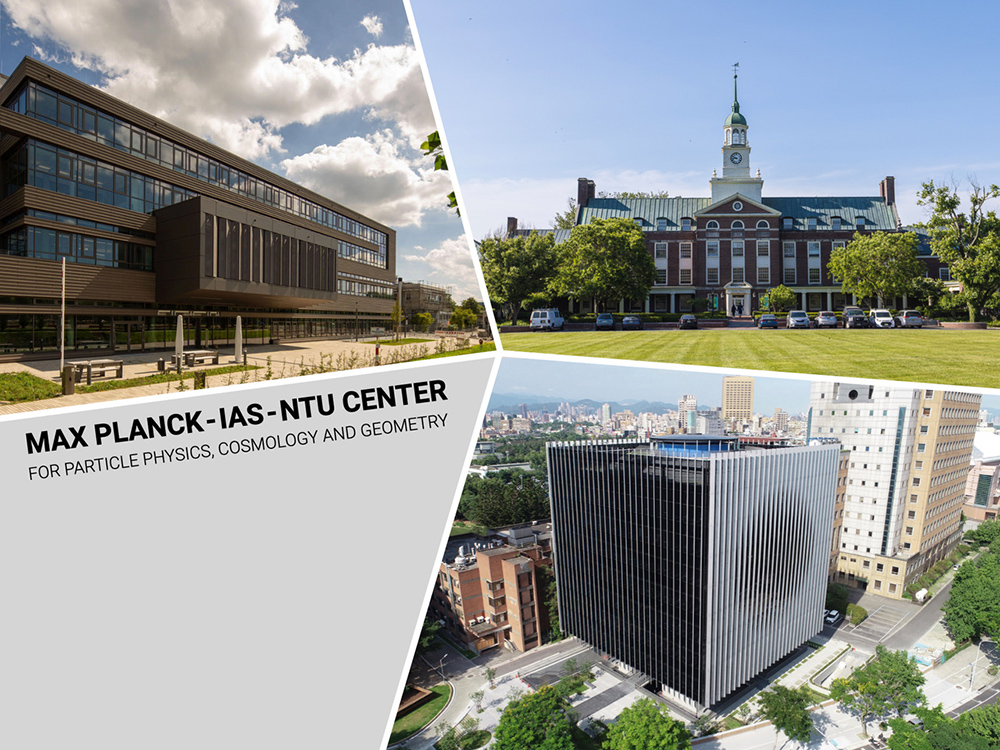
A Distinguished Global Research Center Established at NTU under Trilateral Cooperation
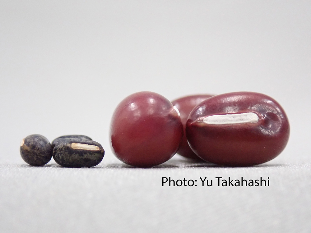
Collaborative study between NTU and Japan uncovers the origin of Adzuki Beans and agriculture in Japan
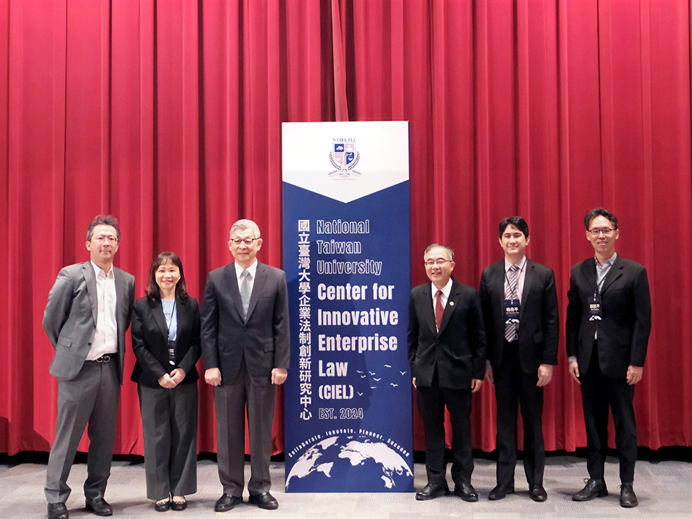
NTU Launches Center for Innovation in Enterprise Law—with Forum Highlighting Trump’s Policy and Legal Shifts Amid Geopolitical Tensions
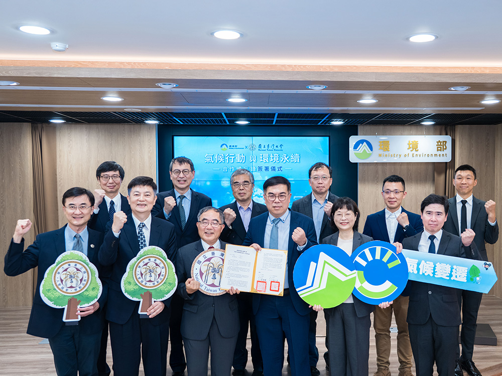
NTU and Ministry of Environment Sign MOU to Advance Net-Zero Transition and Environmental Resilience
Current Spotlights
A new milestone for science at NTU: The inauguration of the Max Planck-IAS-NTU Center
A Distinguished Global Research Center Established at NTU under Trilateral Cooperation
Collaborative study between NTU and Japan uncovers the origin of Adzuki Beans and agriculture in Japan
NTU Launches Center for Innovation in Enterprise Law—with Forum Highlighting Trump’s Policy and Legal Shifts Amid Geopolitical Tensions
NTU and Ministry of Environment Sign MOU to Advance Net-Zero Transition and Environmental Resilience